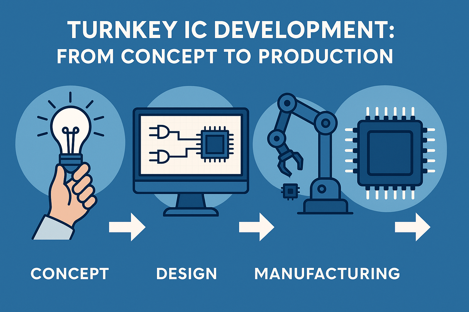
The semiconductor industry continues to evolve at a breakneck pace, creating increasing demand for integrated circuits that meet specific application requirements. Companies seeking custom silicon solutions face a critical decision: partner with a provider who can handle individual stages of development or choose a comprehensive approach. The latter option, known as turnkey IC development, offers end-to-end management that transforms initial concepts into production-ready chips.
Understanding how complete semiconductor solutions work requires examining every phase of the development journey. From specification definition through high-volume manufacturing, each stage demands specialized expertise, advanced tools, and strategic coordination. This comprehensive approach eliminates the complexity of managing multiple vendors while ensuring seamless transitions between development phases.
Understanding Complete Semiconductor Solutions
Complete semiconductor development represents a holistic service model where a single provider manages every aspect of custom chip creation. Unlike traditional approaches that fragment responsibilities across multiple vendors, this methodology centralizes accountability and expertise. Companies benefit from unified project management, consistent quality standards, and streamlined communication throughout the entire development timeline.
The value proposition extends beyond convenience. When engineering teams possess deep experience across all development stages, they make informed decisions during early design phases that prevent costly complications during later production stages. This foresight proves invaluable for companies without internal semiconductor expertise who need guidance navigating complex technical decisions.
The Complete ASIC Lifecycle Journey
Application-Specific Integrated Circuit development follows a structured progression that transforms requirements into manufactured products. The lifecycle begins with extensive consultation to understand system needs, performance targets, power constraints, and cost objectives. This initial phase establishes the foundation for successful outcomes by aligning technical capabilities with business goals.
Specification and Architecture Development
Early development stages focus on translating application requirements into detailed technical specifications. Engineers evaluate tradeoffs between performance, power consumption, die size, and manufacturing costs. Architecture decisions made during this phase influence every subsequent step, making thorough analysis essential. Teams consider process node selection, voltage levels, interface standards, and integration strategies that optimize the final solution.
Comprehensive specification documents serve as contracts between providers and clients, defining functionality, performance parameters, physical characteristics, and testing requirements. These documents prevent misunderstandings while providing clear success criteria that guide development efforts. Regular review sessions ensure specifications remain aligned with project objectives as technical details emerge.
Circuit Design and Verification
Once specifications receive approval, design teams begin detailed circuit implementation. Analog designers create circuits that interface with the physical world, handling signals from sensors, actuators, and communication channels. Digital teams develop logic circuits, memory structures, and control systems that process information according to application requirements. Mixed-signal expertise bridges these domains, ensuring seamless interaction between analog and digital functions.
Simulation and verification consume significant development resources but prove critical for success. Engineers use sophisticated tools to verify functionality, characterize performance across operating conditions, and identify potential failure modes. This rigorous testing during virtual prototyping stages prevents expensive discoveries during physical testing phases.
Physical Implementation
Converting verified circuit designs into physical chip layouts requires specialized knowledge of fabrication processes. Layout engineers arrange transistors, routing channels, and metal layers while adhering to strict design rules that ensure manufacturability. They optimize placement to minimize area, reduce power consumption, and maximize performance while maintaining signal integrity.
Design rule checking, layout versus schematic verification, and parasitic extraction confirm that physical implementations match functional designs. These validation steps catch errors before expensive mask sets get manufactured, protecting project schedules and budgets from unexpected delays.
Transitioning from Design to Production
Moving prototypes into manufacturing represents a critical transition that demands careful planning and execution. This phase validates designs under real-world conditions while establishing production processes that ensure consistent quality at volume. Success requires coordination between design teams, fabrication partners, assembly vendors, and testing operations.
Prototype Fabrication and Evaluation
Initial silicon fabrication produces prototype chips that undergo extensive characterization. Engineering teams measure performance parameters, verify functionality across operating conditions, and compare results against simulation predictions. This evaluation identifies any discrepancies between design intent and physical behavior, informing decisions about production readiness.
Prototype testing often reveals opportunities for optimization that improve yields, reduce power consumption, or enhance performance. Experienced teams leverage these insights to refine designs before committing to high-volume production, maximizing return on development investment.
Production Test Program Development
Manufacturing integrated circuits at scale requires automated testing that screens every device for defects and verifies functionality. Test engineers develop programs that efficiently evaluate each chip while maintaining high quality standards. These programs balance test coverage against cost, ensuring comprehensive validation without excessive testing time that increases production expenses.
Dedicated test facility ASIC operations provide controlled environments where wafer probing and final testing occur under precise conditions. Modern facilities feature climate-controlled clean rooms, advanced test equipment, and automated handling systems that process thousands of devices daily. In-house testing capabilities enable rapid iteration during program development while maintaining security for proprietary designs.
Comprehensive ASIC Production Services
Manufacturing custom integrated circuits involves coordinating multiple specialized operations across the supply chain. Wafer fabrication transforms silicon substrates into completed wafers containing hundreds or thousands of individual chips. Semiconductor foundries operate sophisticated facilities where photolithography, deposition, etching, and other processes create circuit structures layer by layer.
Assembly and Packaging Operations
Completed wafers undergo dicing operations that separate individual chips before assembly into protective packages. Packaging technologies range from traditional plastic encapsulation to advanced multi-chip modules that integrate multiple dies within single packages. Package selection influences thermal performance, electrical characteristics, physical size, and cost, making informed choices essential for optimizing system solutions.
Modern packaging capabilities enable innovative solutions like system-in-package designs that combine chips with passive components or wireless modules. These advanced packaging approaches create compact solutions that would be impossible using discrete components, enabling new product categories and enhanced functionality.
Quality Assurance and Reliability Testing
Production operations include rigorous quality control measures that ensure every shipped device meets specifications. Statistical process control monitors manufacturing parameters, identifying trends that might indicate emerging problems before they affect yields. Reliability testing exposes samples to accelerated stress conditions that predict long-term performance, providing confidence in field reliability.
Comprehensive quality systems maintain detailed records tracking every lot through manufacturing. This traceability enables rapid response if field issues emerge while supporting continuous improvement initiatives that enhance processes over time.
The Value of Full-Cycle IC Development
Partnering with providers who manage complete development cycles delivers numerous advantages compared to coordinating multiple vendors. Single-point accountability eliminates finger-pointing when issues arise, ensuring prompt resolution focused on project success rather than liability assignment. Unified teams share knowledge across development phases, making informed decisions that prevent downstream complications.
Cost predictability improves when single providers quote comprehensive services. Companies receive clear budgets covering all development stages rather than discovering unexpected expenses as projects progress through fragmented supply chains. Schedule reliability similarly benefits from coordinated planning that anticipates dependencies and allocates resources efficiently.
Expertise That Spans Decades
Successful custom chip development requires deep expertise accumulated through hundreds of completed projects. Engineering teams must understand subtle interactions between design choices and manufacturing realities that only emerge through extensive experience. This knowledge base enables creative problem-solving when challenges arise, finding solutions that less experienced teams might miss.
Providers with long operational histories have established relationships with fabrication partners, assembly vendors, and component suppliers. These networks provide access to capacity during tight allocation periods while enabling favorable terms that benefit customers through reduced costs and improved service.
Making Strategic Decisions About Custom Silicon
Companies considering custom integrated circuits face important decisions about development approaches and partner selection. Understanding the complete lifecycle helps evaluate options and choose strategies aligned with business objectives. Comprehensive providers offer advantages for organizations without internal semiconductor expertise or those seeking simplified vendor management.
The economics of custom chip development continue improving as design tools advance and manufacturing processes mature. Return on investment calculations should consider not just unit cost reductions but also benefits like reduced board space, improved reliability, enhanced intellectual property protection, and optimized performance. These factors often justify development costs even for moderate production volumes.
Frequently Asked Questions
What distinguishes complete semiconductor development from traditional approaches?
Complete solutions centralize all development activities under single management, eliminating coordination challenges inherent in multi-vendor approaches. This integration ensures consistent quality, simplified communication, and unified accountability throughout project lifecycles. Customers benefit from single-point contact rather than managing relationships with separate design, fabrication, assembly, and testing vendors.
How long does custom chip development typically require?
Development timelines vary based on complexity, ranging from six months for straightforward designs to over twelve months for sophisticated systems. Factors influencing schedules include circuit complexity, verification requirements, process node selection, and prototype iteration needs. Following prototype evaluation, production release typically requires two to four additional months for test program completion and manufacturing qualification.
What cost factors should companies consider when evaluating custom silicon?
Total cost analysis includes non-recurring engineering expenses for development, mask set costs, prototype fabrication, and production unit pricing. However, companies should also consider savings from reduced bill of materials costs, smaller circuit boards, simplified assembly, improved reliability, and enhanced intellectual property protection. Most projects achieve positive returns within twelve to eighteen months of full production.
How do providers ensure designs meet manufacturing requirements?
Experienced teams apply design-for-manufacturing principles throughout development, making choices that optimize production yields. They select appropriate process nodes, follow foundry design rules, implement robust circuits tolerant of process variations, and leverage proven intellectual property blocks. Close relationships with fabrication partners provide insights into manufacturing capabilities that inform design decisions.
What advantages come from in-house testing capabilities?
Dedicated testing facilities enable rapid program development iteration, maintain security for proprietary designs, and provide complete control over quality standards. On-site operations eliminate shipping delays and communication challenges associated with offshore testing while enabling close collaboration between design and test engineering teams. This integration accelerates problem resolution and supports continuous improvement initiatives.
Can development schedules be accelerated if business needs change?
Most fabrication and assembly partners accommodate expedited processing for additional fees. Providers with strong supplier relationships can often arrange priority scheduling when customers require faster delivery. However, acceleration requests work best when communicated early, allowing suppliers to reserve capacity and adjust production schedules accordingly.
Conclusion
The semiconductor industry’s complexity makes complete development solutions increasingly attractive for companies seeking custom integrated circuits. By partnering with experienced providers who manage entire lifecycles, organizations simplify vendor relationships while benefiting from deep expertise that spans design through production. This approach delivers predictable costs, reliable schedules, and high-quality results that meet demanding application requirements across diverse markets.
Success in custom silicon development requires more than technical capability. It demands proven processes, established supplier networks, comprehensive testing infrastructure, and decades of experience solving unique challenges. Companies choosing complete solution providers gain access to these resources without building internal capabilities, accelerating time to market while minimizing technical risks. As applications continue demanding increasingly specialized functionality, comprehensive semiconductor development services will remain essential for innovation across industries.
About Custom Silicon Solutions
Custom Silicon Solutions represents the pinnacle of Turnkey IC Solutions, delivering comprehensive semiconductor development services that transform concepts into production-ready integrated circuits. Founded nearly three decades ago on the principle that innovative circuit solutions emerge from exceptional engineering talent, the company has established itself as a premier provider of custom ASIC development and manufacturing services.
Located in Irvine, California, Custom Silicon Solutions operates from a state-of-the-art 30,000 square foot facility that serves as a complete one-stop-shop for custom semiconductor needs. The company specializes in analog, mixed-signal, high-voltage, and wireless communication circuits, bringing deep technical expertise to challenging applications across industrial, medical, aerospace, defense, and consumer markets.
What truly distinguishes Custom Silicon Solutions is the remarkable depth of engineering experience within the organization. The average engineer maintains over 25 years of integrated circuit design experience, enabling the team to deliver the most creative and efficient solutions in the industry. This extensive experience base spans circuit design, system architecture, and application expertise, allowing engineers to address unique technical challenges with proven methodologies and innovative approaches.
The company has successfully completed over 300 ASIC designs throughout its history, demonstrating consistent ability to deliver complex semiconductor solutions across diverse technology nodes and application requirements. This track record reflects not only technical capability but also the robust processes and quality systems that ensure reliable project execution from initial consultation through high-volume production.
Custom Silicon Solutions maintains complete control over critical production operations through its owned and operated 8,000 square foot class 10,000 clean room test facility. This dedicated space houses both wafer probing and final package testing operations, providing the infrastructure necessary to validate designs and screen production devices under controlled conditions. In-house testing capabilities enable rapid iteration during test program development while maintaining security for proprietary customer designs.
The company’s comprehensive service model covers every phase of the development journey. Engineering teams handle specification development, translating customer requirements into detailed technical documentation. Circuit designers implement functionality using proven design methodologies and sophisticated simulation tools. Layout specialists create physical implementations optimized for manufacturability and performance. Test engineers develop production screening programs that balance coverage against efficiency. Project managers coordinate activities across fabrication partners, assembly vendors, and internal operations to ensure seamless execution.
While Custom Silicon Solutions operates as a fabless semiconductor company, the organization has cultivated strong relationships with leading wafer fabrication foundries, assembly houses, and component suppliers worldwide. This established ecosystem enables optimal technology selection for each project while providing access to manufacturing capacity even during periods of tight industry allocation. The company’s fab-agnostic approach ensures customers receive solutions optimized for their specific requirements rather than being constrained by single-source manufacturing relationships.
From initial concept discussions through mass production management, Custom Silicon Solutions delivers the expertise, infrastructure, and support necessary for successful custom integrated circuit development. The company’s three-decade history demonstrates sustained commitment to engineering excellence, customer success, and innovation in semiconductor technology.