Modern electronic systems demand seamless interaction between the physical world and digital processing engines. Sensors capture temperature, pressure, light, and countless other parameters as analog signals that require conditioning before digital systems can interpret them. Actuators need carefully controlled voltages and currents to operate motors, displays, and communication interfaces. Between these domains lies a critical technology: mixed-signal ASICs that unite analog and digital functionality on single integrated circuits.
The evolution of semiconductor technology has enabled increasingly sophisticated integration that places diverse circuit types onto unified silicon substrates. Engineers can now design chips containing sensitive analog amplifiers alongside high-speed digital processors, power management circuits coexisting with delicate sensing elements, and high-voltage drivers integrated with low-voltage logic. This convergence creates opportunities for system architects to reimagine product designs while addressing challenges that emerge when combining fundamentally different circuit types.
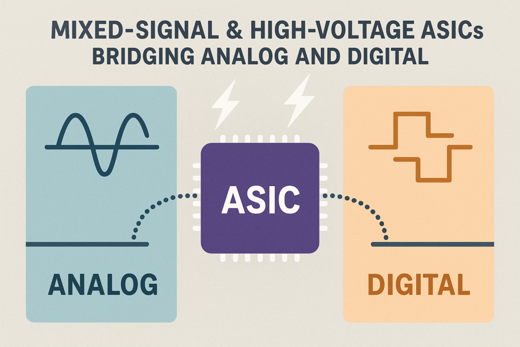
Understanding Dual-Domain Integration
Traditional electronic systems separated analog and digital functions across multiple chips connected through circuit boards. Analog circuits conditioned signals from sensors, converting physical phenomena into electrical representations. Separate analog-to-digital converters bridged domains, feeding processed information to digital processors. Additional components handled power management, output driving, and interface functions. This distributed architecture consumed board space, increased component costs, and created potential reliability issues through numerous interconnections.
Integration transforms this paradigm by unifying functions within single devices. When analog digital integration occurs on common substrates, systems benefit from reduced size, lower component counts, decreased assembly costs, and improved reliability through fewer interconnections. Performance often improves as well, since signals travel shorter distances between circuit blocks, minimizing parasitic effects and electromagnetic interference that plague board-level implementations.
However, achieving successful integration requires overcoming substantial technical challenges. Analog circuits operate in continuous voltage and current domains, responding to subtle signal variations that carry information. Digital circuits switch between discrete states, creating electrical noise that can corrupt sensitive analog signals. Power supply requirements differ dramatically—digital logic thrives on low voltages that maximize speed and minimize power, while analog amplifiers often need higher voltages for adequate signal swing. High-voltage circuits introduce additional complications, requiring specialized transistor structures and layout techniques that prevent breakdown while maintaining isolation from sensitive low-voltage components.
The Architecture of Mixed-Signal Chip Design
Successful dual-domain implementations require careful planning during architectural development. Engineers partition functionality between analog and digital domains based on signal characteristics, processing requirements, and performance objectives. This partitioning influences every subsequent design decision, making thorough analysis during early project phases essential for optimal outcomes.
Analog Domain Responsibilities
Analog circuits interface directly with physical sensors and actuators, handling signal conditioning that prepares information for digital processing. Amplifiers boost weak signals from photodiodes, thermocouples, strain gauges, and capacitive sensors to levels suitable for conversion. Filters remove unwanted frequency components that represent noise or interference. Comparators make threshold decisions that detect specific signal conditions. Reference circuits generate stable voltages and currents that establish measurement baselines.
These analog blocks demand exceptional precision and stability across operating conditions. Temperature variations, supply voltage fluctuations, and process variations during manufacturing all influence analog performance. Experienced designers employ circuit techniques that minimize sensitivity to these variations, using matched transistor pairs, common-centroid layouts, and feedback architectures that enhance stability. Component selection balances competing requirements for accuracy, speed, power consumption, and silicon area.
Digital Processing Excellence
Digital sections implement complex algorithms that extract meaning from converted analog signals. Microprocessor cores execute software that makes decisions based on sensor inputs. State machines coordinate operations across multiple system functions. Memory blocks store calibration coefficients, configuration parameters, and temporary data. Interface circuits communicate with external devices through standardized protocols.
Digital designers optimize circuits for specific performance metrics. Low-power applications minimize switching activity and clock frequencies while employing power management techniques like clock gating and voltage scaling. High-performance systems maximize throughput through pipelining and parallel processing. Area-constrained designs share resources and minimize memory requirements. Each optimization strategy requires different architectural choices and implementation techniques.
The Critical Conversion Interface
Analog-to-digital and digital-to-analog converters form bridges between domains, translating between continuous and discrete representations. These converters profoundly influence overall system capability, with resolution, speed, linearity, and noise performance determining what signals systems can accurately process.
Successive approximation converters offer balanced performance for moderate-speed applications, combining reasonable resolution with efficient power consumption. Delta-sigma architectures achieve exceptional resolution for lower-frequency signals through oversampling and noise shaping. Pipeline converters deliver high speeds necessary for video and communication applications. Each topology presents distinct tradeoffs that designers evaluate against application requirements.
High-Voltage IC Design Considerations
Many applications require voltages far exceeding those used by standard digital logic. Motor controllers need tens or hundreds of volts to drive actuators. Display drivers generate elevated voltages for liquid crystal and electrophoretic panels. Power management circuits convert between widely different voltage domains. Medical devices deliver controlled electrical stimulation. Automotive systems withstand harsh electrical environments while managing substantial power levels.
Specialized Process Technologies
High-Voltage ASIC Services leverage specialized manufacturing processes that extend beyond standard complementary metal-oxide-semiconductor technologies. These processes include additional transistor structures capable of withstanding elevated voltages without breakdown. Junction isolation techniques separate high-voltage circuits from sensitive low-voltage components. Thick oxide layers insulate gates handling substantial voltages. Deep trenches or buried layers provide vertical isolation that prevents high-voltage signals from affecting adjacent circuits.
Bipolar-CMOS-DMOS processes combine traditional bipolar transistors, standard CMOS logic, and double-diffused metal-oxide-semiconductor power devices on common substrates. This integration enables complete power management systems including high-voltage switches, precision analog circuits, and sophisticated digital control within single chips. The manufacturing complexity increases compared to standard processes, requiring additional masking steps and careful process control, but the integration benefits justify these requirements for appropriate applications.
Layout and Protection Strategies
High-voltage circuits demand meticulous physical implementation that prevents electrical breakdown while managing heat dissipation. Layout engineers maintain adequate spacing between conductors carrying different voltages, following design rules that account for field strength limitations. Guard rings surround high-voltage circuits, providing defined current paths that prevent latch-up conditions. Metal layers distribute heat generated by power-handling devices, often connecting to package leads that conduct thermal energy away from silicon.
Electrostatic discharge protection becomes increasingly important at elevated voltages. Specialized structures clamp voltage spikes that could otherwise destroy sensitive circuits during handling or operation. These protection devices must activate quickly when dangerous voltages appear while remaining transparent during normal operation, requirements that demand careful design and characterization.
Applications Driving Dual-Domain Innovation
Custom mixed-signal solutions address diverse application needs across numerous industries. Each market segment presents unique requirements that influence design priorities and implementation strategies.
Industrial Automation and Control
Factory automation systems monitor countless parameters—temperature, pressure, flow, position, vibration—using sensors distributed throughout facilities. Integrated circuits combine sensor interfaces, signal processing, communication protocols, and control algorithms that coordinate complex operations. These chips often operate in harsh environments with wide temperature ranges, electromagnetic interference, and mechanical stress, requiring robust designs that maintain specifications under challenging conditions.
Motor control represents particularly demanding applications where high-voltage drivers deliver substantial currents while precision analog circuits measure position feedback and digital processors execute control algorithms at high rates. The integration enables compact motor control modules that reduce system complexity while improving performance through tight coupling between sensing, processing, and actuation functions.
Medical Device Innovation
Healthcare applications impose stringent requirements for safety, reliability, and performance. Implantable devices demand ultra-low power operation that maximizes battery life while delivering therapeutic functions like cardiac pacing or neural stimulation. These systems integrate high-voltage stimulation circuits alongside sensitive biopotential amplifiers, wireless communication blocks, and sophisticated power management—all within miniature packages that minimize patient impact.
Diagnostic equipment processes signals from diverse sensors including electrodes, ultrasonic transducers, and optical detectors. The signal conditioning requirements span from microvolt biopotentials to high-frequency ultrasound echoes, demanding exceptional dynamic range and noise performance. Integration improves measurement quality by reducing parasitic effects while simplifying instrument design.
Automotive Electronics Evolution
Modern vehicles contain hundreds of electronic control units managing propulsion, safety, comfort, and entertainment systems. Many automotive chips operate in electrically noisy environments while handling substantial power levels and wide temperature ranges. Battery management systems monitor cell voltages and currents, balancing charge distribution across large battery packs in electric vehicles. Motor controllers deliver kilowatts to traction motors with precise current regulation. Sensor interfaces process signals from cameras, radar, and lidar that enable advanced driver assistance.
The automotive qualification requirements extend beyond typical commercial specifications, demanding extensive reliability testing and stringent quality controls. Chips must survive temperature cycling, mechanical shock, electromagnetic compatibility testing, and long-term aging validation that ensures decade-long operational lifetimes.
The Value of Comprehensive Development Services
Developing sophisticated Mixed-Signal / High-Voltage ICs requires specialized expertise that extends beyond traditional circuit design capabilities. Organizations offering comprehensive services provide value through deep experience accumulated across numerous projects and diverse applications.
Specialized Design Knowledge
Complex dual-domain chips demand engineers who understand subtle interactions between circuit types that share common substrates. These specialists recognize how digital switching noise couples into analog signals through supply rails, substrate currents, and electromagnetic radiation. They employ partitioning strategies that isolate sensitive circuits from noise sources. They design power distribution networks that provide clean supplies to analog blocks while accommodating digital switching currents. They implement grounding schemes that minimize ground bounce without creating problematic current loops.
High-voltage expertise encompasses understanding breakdown mechanisms, creating reliable isolation structures, and designing protection circuits that safeguard devices during fault conditions. Engineers leverage simulation tools that model electrical stress, thermal effects, and reliability degradation mechanisms. This analysis informs decisions about device sizing, layout geometry, and operating conditions that ensure long-term reliability.
Process Technology Selection
Choosing appropriate manufacturing processes profoundly influences chip capability, cost, and development schedule. Experienced providers maintain relationships with foundries offering diverse process options, enabling optimal technology selection for each project. They understand process capabilities, design rule requirements, and available device structures. This knowledge guides architectural decisions during early project phases, preventing costly redesigns that might otherwise emerge during implementation.
Some applications benefit from advanced processes offering minimum feature sizes that maximize digital performance and density. Others prioritize analog precision available in mature processes with excellent device matching. High-voltage requirements may dictate specialized processes unavailable at leading-edge nodes. Navigating these tradeoffs requires understanding both application requirements and process capabilities.
Verification and Validation Excellence
Dual-domain chips present verification challenges that exceed those of purely digital implementations. Analog circuits require extensive simulation across process corners, voltage ranges, and temperature extremes. High-voltage portions need careful characterization that confirms breakdown margins and validates protection mechanisms. Mixed-signal verification must address interactions between domains, ensuring digital noise doesn’t corrupt analog performance.
Silicon validation extends verification to physical devices, characterizing actual performance against simulated predictions. Experienced teams develop efficient test strategies that thoroughly evaluate functionality while maintaining reasonable testing costs. They leverage statistical methods that predict production yields and identify opportunities for design optimization.
Frequently Asked Questions
What advantages does integration provide compared to discrete implementations?
Integrating analog and digital functions onto single chips reduces component counts, decreases board space requirements, lowers assembly costs, and improves reliability through fewer interconnections. Performance often improves as signals travel shorter distances, minimizing parasitic effects. Systems become more compact, consume less power, and achieve better electromagnetic compatibility. Cost advantages typically justify development expenses when production volumes exceed modest thresholds.
How do designers prevent digital noise from corrupting analog signals?
Multiple techniques isolate sensitive analog circuits from digital switching noise. Physical separation on chip layouts increases distance between noise sources and sensitive nodes. Separate power supplies feed analog and digital sections, preventing coupling through supply rails. Guard rings and substrate contacts provide controlled return paths for substrate currents. Careful grounding schemes minimize ground bounce. Quiet digital design practices reduce switching noise generation. Shielding techniques protect sensitive traces from electromagnetic coupling.
What process technologies support high-voltage integration?
Specialized bipolar-CMOS-DMOS processes combine standard logic with high-voltage transistors capable of withstanding elevated potentials. These technologies include additional device structures, thick oxide layers for gate insulation, and isolation techniques that separate high-voltage circuits from sensitive components. Voltage capabilities range from tens to hundreds of volts depending on specific process offerings. Process selection balances voltage requirements against digital performance needs and analog precision specifications.
How long does dual-domain chip development require?
Development timelines depend on complexity, ranging from six months for straightforward implementations to over twelve months for sophisticated systems. Analog and high-voltage portions often consume more development time than digital sections due to iterative optimization and extensive corner simulations. Prototype evaluation periods vary based on characterization requirements. Production qualification adds several months for test program development and manufacturing setup.
What applications most benefit from integrated solutions?
Industrial sensor interfaces, motor controllers, power management systems, medical devices, automotive electronics, and consumer products all leverage dual-domain integration. Applications processing signals from physical sensors while requiring sophisticated digital processing particularly benefit. Systems demanding compact implementations, low power operation, or cost reduction through part consolidation make ideal candidates. Markets accepting moderate development costs while producing sufficient volumes to amortize expenses see attractive returns.
How do high-voltage capabilities expand application possibilities?
High-voltage integration enables direct interfaces to motors, displays, and actuators without external driver components. Power management systems efficiently convert between voltage domains while maintaining regulation. Medical devices deliver therapeutic stimulation at appropriate energy levels. Automotive systems withstand harsh electrical environments while managing substantial power. The voltage range expansion allows single chips to handle complete signal chains from sensors through processing to actuation, maximizing integration benefits.
Conclusion
The convergence of analog, digital, and high-voltage circuit techniques onto unified silicon platforms represents one of semiconductor technology’s most enabling developments. Dual-domain integration creates opportunities for system architects to reimagine electronic products, reducing size and cost while improving performance and reliability. However, successfully combining fundamentally different circuit types demands specialized expertise accumulated through extensive experience across diverse applications.
Organizations seeking custom integrated circuits that bridge analog and digital domains benefit from partnering with providers possessing comprehensive capabilities spanning circuit design, process technology, layout implementation, and production testing. These partnerships deliver optimized solutions that meet demanding requirements while navigating the complex tradeoffs inherent in dual-domain implementations.
As applications continue demanding more sophisticated functionality within increasingly constrained packages, the importance of advanced integration will only grow. The ability to seamlessly unite analog sensing, digital processing, and high-voltage actuation within single chips enables innovation across industries from industrial automation through medical devices to automotive electronics. Success in these endeavors requires not just technical capability but proven processes, established manufacturing relationships, and deep understanding of how circuit techniques combine to create reliable, high-performance solutions.
About Custom Silicon Solutions: Your Mixed-Signal ASIC Partner
Custom Silicon Solutions has established itself as the industry’s premier provider of Turnkey IC Solutions, with particular distinction in analog, mixed-signal, and high-voltage ASIC development. For nearly three decades, the company has specialized exclusively in bridging the analog and digital domains, delivering sophisticated integrated circuits that seamlessly unite diverse circuit technologies on single silicon substrates. This focused expertise has made Custom Silicon Solutions the partner of choice for organizations requiring complex dual-domain integration across industrial, medical, aerospace, defense, and consumer applications.
Operating from a state-of-the-art 30,000 square foot facility in Irvine, California, Custom Silicon Solutions has built its reputation on unmatched analog and mixed-signal circuit design capabilities. The company’s engineering team averages over 25 years of integrated circuit design experience specifically in the challenging realm where analog precision meets digital sophistication. This depth of mixed-signal expertise enables the team to navigate the intricate challenges of combining sensitive analog amplifiers with high-speed digital processors, high-voltage power circuits with delicate low-voltage logic, and precision sensor interfaces with sophisticated signal processing algorithms.
The company’s core strength lies in understanding the subtle interactions that occur when fundamentally different circuit types share common silicon substrates. Custom Silicon Solutions’ engineers excel at partitioning functionality between analog and digital domains, implementing isolation strategies that prevent digital switching noise from corrupting sensitive analog signals, and designing power distribution networks that simultaneously satisfy the conflicting requirements of both domains. This specialized knowledge proves invaluable for applications demanding exceptional analog performance alongside complex digital processing.
Custom Silicon Solutions’ mixed-signal capabilities span the complete spectrum of dual-domain integration challenges. Analog specialists design precision amplifiers achieving microvolt-level sensitivity, filters implementing sophisticated frequency shaping, voltage references providing sub-ppm stability, and sensor interfaces extracting maximum performance from diverse transducers. Digital experts implement signal processing algorithms, communication protocols, control state machines, and embedded memory structures. High-voltage designers create robust power management circuits, motor drivers handling hundreds of volts, and stimulation systems delivering precise energy while maintaining isolation from sensitive components.
The organization maintains an 8,000 square foot class 10,000 clean room dedicated to mixed-signal production testing operations. This facility performs both wafer-level probing and final package testing with specialized equipment configured for the unique challenges of dual-domain validation. Testing mixed-signal chips requires simultaneous verification of analog performance parameters—linearity, noise, offset, gain accuracy—alongside digital functionality and timing specifications. The in-house capabilities enable Custom Silicon Solutions to develop comprehensive test strategies that efficiently screen devices while maintaining the stringent quality standards essential for analog precision.
Custom Silicon Solutions’ comprehensive service model addresses every phase of mixed-signal ASIC development from initial concept through high-volume manufacturing. Architecture consultations help clients partition system functionality optimally between analog and digital domains while selecting appropriate process technologies that balance analog performance against digital capability and high-voltage requirements. Circuit designers implement solutions using proven mixed-signal design methodologies, extensive corner simulations that validate performance across operating conditions, and sophisticated noise analysis that ensures domain isolation. Layout specialists create physical implementations employing matched device structures for analog precision, careful power distribution that separates analog and digital supplies, and proper guard ring placement that prevents substrate coupling.
With over 300 completed ASIC designs spanning diverse mixed-signal applications, Custom Silicon Solutions brings proven execution capabilities specifically focused on dual-domain integration challenges. The company’s established relationships with foundries offering specialized bipolar-CMOS-DMOS and other mixed-signal process technologies enable optimal selection for each project’s unique combination of analog precision, digital performance, and voltage handling requirements. This focused expertise in mixed-signal development, combined with comprehensive in-house testing infrastructure and proven project management methodologies, positions Custom Silicon Solutions as the ideal partner for organizations seeking to transform system architectures through sophisticated analog-digital integration that delivers competitive advantages in size, cost, performance, and reliability.